A 0.42-Nanometer Breakthrough Could Push Transistors Beyond Silicon
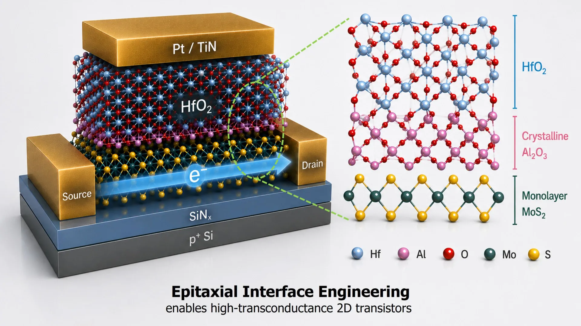
Researchers from National Yang Ming Chiao Tung University and TSMC have developed a 0.42-nanometer interface layer that addresses a major engineering hurdle for two-dimensional semiconductors. By engineering the atomic boundary between the semiconductor and the gate dielectric, the team achieved high electrical control without sacrificing charge carrier mobility. This breakthrough is significant for the semiconductor industry as it provides a viable path for scaling transistors beyond the physical limits of conventional silicon.
The research, published in Nature Electronics, focuses on the gate dielectric layer, which controls electron movement in transistors. While atomically thin semiconductors like molybdenum disulfide (MoS2) offer potential for smaller and faster devices, adding insulating layers often disrupts the material interface, leading to electron scattering and performance loss. To solve this, the team from National Yang Ming Chiao Tung University (NYCU) and TSMC Corporate Research applied an ultrathin epitaxial aluminum layer directly onto CVD-grown monolayer MoS2, which was then carefully oxidized to create a 0.42-nanometer aluminum oxide buffer.
This engineered interface serves two critical functions: it provides a smooth, continuous surface for the subsequent growth of a high-k hafnium oxide dielectric and acts as an atomic buffer to limit unwanted electrical interactions. The resulting short-channel top-gate transistors achieved an equivalent oxide thickness of approximately one nanometer. Technical testing revealed impressive performance metrics, including low leakage current, minimal hysteresis, and a maximum transconductance of 0.45 mS μm-1 in devices with channels measuring approximately 100 nanometers.
Unlike many previous experiments that relied on mechanically exfoliated flakes, this study utilized wafer-scale chemical vapor deposition (CVD) grown MoS2, making the process more compatible with industrial manufacturing standards. Professors Wen-Hao Chang and Tsung-En Lee noted that as components reach atomic dimensions, the interface itself becomes a functional part of the device rather than just a boundary. This shift toward interface engineering offers a new strategy for the semiconductor industry to pursue low-power logic and advanced electronic systems as traditional silicon scaling reaches its physical limits.
Summary generated by RabbitReport AI from public reporting. The full article and original reporting belong to ScienceDaily.