The Latest News In IC Packaging & Test
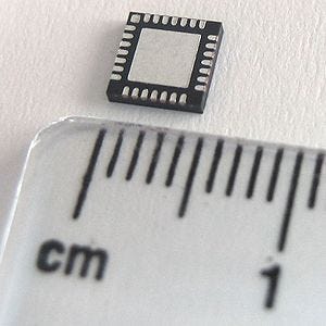
The semiconductor packaging sector is experiencing a significant wave of expansion and technological advancement, particularly as China and India bolster their domestic capabilities. China's leading firms are investing billions into 3D system integration and high-bandwidth memory, while India is rapidly emerging as a global hub for outsourced semiconductor assembly and test services. These developments reflect a broader industry shift toward advanced packaging solutions to meet the demands of the automotive, communications, and artificial intelligence markets.
China is aggressively expanding its advanced packaging infrastructure through major projects from its leading domestic firms. JCET, the country's largest outsourced semiconductor assembly and test (OSAT) provider, recently inaugurated a new facility for high-density 3D system integration at its Jiangyin manufacturing base. Simultaneously, SJ Semiconductor (SJSemi) has announced the Dongsheng Hexin 3D Integrated Chip Manufacturing Project, a new advanced packaging plant focused on 3D multi-chip packaging technologies. This project involves a total investment of approximately RMB 10 billion (US$1.37 billion) and follows SJSemi's successful IPO on the Shanghai Stock Exchange STAR Market, which raised over US$733 million.
In the memory sector, China's sole DRAM supplier, CXMT, is working to develop high-bandwidth memory (HBM) to compete with global peers. While international competitors are moving toward HBM4, CXMT is currently in the early stages of HBM3, which offers significantly less bandwidth per stack than the upcoming generation. According to analysts at TD Cowen, CXMT faces substantial hurdles regarding yield, density, and bandwidth. However, if the company successfully ramps up HBM3 and HBM3E production, it could pose a risk to the global memory market, depending on the sustained strength of AI-driven demand.
India is also reaching major milestones in its bid to become a chip-packaging and test hub. CG Semi, a joint venture between CG Power and Industrial Solutions, Renesas, and Stars Microelectronics, has officially started production at its G1 OSAT facility in Gujarat. This is the first of two planned facilities, with the joint venture investing over US$795.06 million over five years. The facility is designed to produce QFN and QFP packages, as well as flip-chip BGA and CSP packages, for applications ranging from consumer electronics to the automotive and industrial sectors.
The global ecosystem is seeing further consolidation and strategic shifts as manufacturers optimize their footprints. On Semiconductor (onsemi) has entered into definitive agreements to divest two of its manufacturing facilities as part of its planned divestiture strategy. Other notable activity in the sector includes Solstice's acquisition of Element and the formation of new joint ventures focused on glass core technologies. These moves highlight the complex and fast-moving nature of the IC packaging and test business as companies race to support the next generation of semiconductor applications.
Summary generated by RabbitReport AI from public reporting. The full article and original reporting belong to Semiecosystem.